Inside the Cloudlifter.
Explore a balanced microphone booster, build your understanding from board to enclosure, and test what changes the signal.
Start the lesson →The lesson home could not load. The workshop and downloadable lessons remain available.
Open the Cloudlifter workshop →Download the lesson manuscriptBuild the Cloudlifter circuit.
A 3D build-along for the CL-1’s balanced JFET circuit.
Hardware untested · local prototype
Explore the input stage.
Inspect the parts. Follow the signal.
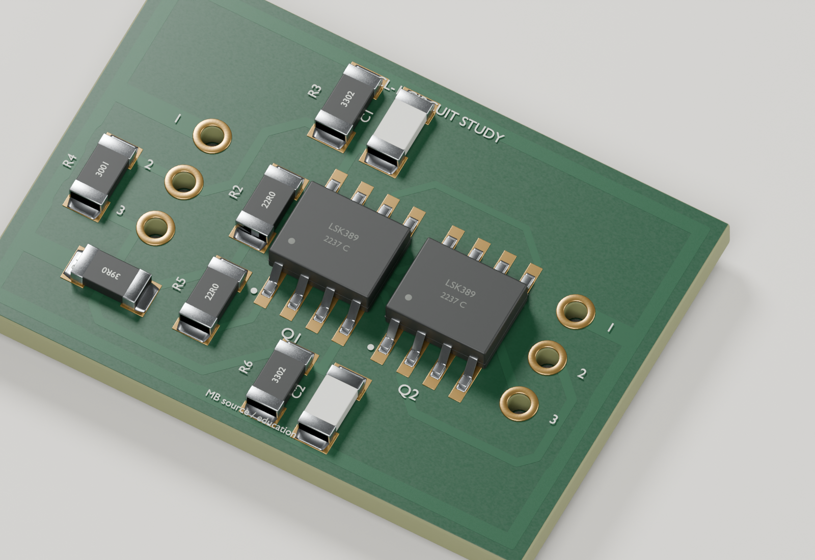
The 3D model is unavailable. The rendered reference and lesson remain available.
Separate
Separation reveals the installed components.
Saved reference waveform
Loading study…The saved waveform could not load.
Make the joint. Test the circuit.
Loading the assembly exercise…
The assembly exercise could not load.
Open the Cloudlifter →Inside the Cloudlifter workshop.
A 44-second introduction to this workshop. Continue into the eight guided chapters to inspect, build and test the circuit.
See what powers the signal.
Predict a change. Compare the evidence. Follow the connection back to the circuit.
Calculated behavior · hardware unmeasured
Choose an experiment for a guided comparison, or change the bench settings yourself.
The simulation data could not load. The circuit diagram and source tables are still available.
Open circuit & connections →What changed
The assembled PCB
Loading 3D…
3D is unavailable. The still, waveform studies and numeric probes remain usable.
Electrons drift from the grounded return toward the output drains, opposite to conventional current. Their movement is greatly enlarged and time-scaled; signal energy does not travel at this drift speed.
The virtual bench
P48 onSettings follow this experiment. Choose Explore freely to change them yourself.
- Fundamental gain
- —
- Output peak
- —
- Phantom draw · DC
- —
- Output DC · each leg
- —
Compare with a baseline
Keep a result, then change one setting to compare.
| Reading | Baseline | Current | Change |
|---|
Input and output each use their own voltage scale.
Input / output
4 cycles · independent voltage scalesRead at the cursor
Select a point on the plot, use the Time slider, or enter a time. Seeking pauses playback.
| Signal | Baseline · dashed | Current · solid |
|---|---|---|
| Input | — | |
| Output | — |
Signed voltages use linear interpolation between saved SPICE samples. Time is relative to the start of each four-cycle excerpt. CSV keeps each case’s original samples and times.
Small-signal response
Follow the selected connections
Q1Choose a symbol, select a part on the PCB, or use the probe menu. Both sections of a selected JFET package light together.
Loading the connection drawing…
Read the highlighted route
Accent wires share a source net with the selected part. Highlighting shows connectivity, not current magnitude.
The two 6.81 kΩ phantom feeds belong to the receiving interface. The microphone signal enters at J2; power arrives at J3.
Open the complete pad table →The linked drawing could not load. Open circuit & connections or .
Model assumptions, source files & what the motion means
The circuit follows the pinned MostlyBuilds teardown PCB. Four matched JFET sections use an ngspice level-1 adaptation of Linear Systems’ LSK389C Rev 2 parameters. The model assumes 27 °C, matched devices, matched 6.81 kΩ feed resistors, a resistive 150 Ω balanced microphone source, and an interface load coupled through two ideal 47 µF capacitors. Those capacitors belong to this virtual interface, outside the booster.
Every control combination selects a saved nonlinear SPICE run. The model omits device mismatch, component tolerances, microphone inductance, noise, RF/EMC, breakdown, thermal effects and wiring parasitics. Unsupported vendor parameters ISR, NR, ALPHA and VK are omitted. Calculated voltages and gain are study results, not safe bench limits or measurements of a Cloudlifter.
Copper paths follow the source tracks and ground pour. The line across a package is a dashed explanation of channel conduction; the die has not been modeled. Ground-pour motion shows a possible return route, not a solved current-density field. Particle size, spacing and speed are illustrative. AC mode shows local back-and-forth motion at the gates, not electrons flying through the gate into the output. The JFET channel current is supplied by phantom power.
Follow the actual connections.
The source-derived pad table is the authority for this model. Connect XLRs by their actual contact numbers; mating and solder views are mirrored.

Two packages, four JFETs
Q1 contains the input sections; Q2 contains the cascode sections. Follow each source and drain connection in the table below. A cascode is different from two complete amplifiers in cascade.
Power arrives at the output
The interface sends phantom DC on output pins 2 and 3, with a return on pin 1. Its feed resistors also influence the gain load.
RF shunts at the input
C1 and C2 each connect an input leg to ground. They are not series DC-blocking capacitors.
Download the complete pad table ↗Inspect the original KiCad project ↗XLR connections
| Board pad | Connector | Contact |
|---|---|---|
| J2.1 | Female input | 1 · screen |
| J2.2 | Female input | 2 · hot |
| J2.3 | Female input | 3 · cold |
| J3.1 | Male output | 1 · screen |
| J3.2 | Male output | 2 · hot |
| J3.3 | Male output | 3 · cold |
SOIC package pins
| Pin | Function |
|---|---|
| 1 / 2 / 4 | S1 / D1 / G1 |
| 5 / 6 / 8 | S2 / D2 / G2 |
| 3 / 7 | Substrate · floating in source |
Check the datasheet for the exact ordered part. The TO-71 package has a different mapping.
Show all source pad nets
| Part | Pad | Net |
|---|
Put every part in its place.
Ten electronic components, two header connections, and the mechanical assembly. Values below follow the source schematic and teardown list.
The schematic and teardown specify LSK389C. The PCB value strings and reused library metadata still say LSK389B. This course uses C and preserves the discrepancy in the research notes.
| Reference | Value | Package | Role |
|---|
Tools and supplies
Magnification, fine tweezers, temperature-controlled soldering equipment, flux and cleaning materials; a multimeter; suitable DC-safe audio test equipment; a protected P48 fixture and support from someone comfortable with electronics for first power.
Mechanical parts
Female input XLR, male output XLR, suitable metal housing, insulation, wire and fixings. The virtual enclosure is illustrative. Use the actual connector and housing drawings to check fit.
Know what each source proves.
Manufacturer specifications, a patent disclosure, and a direct teardown support different claims. This workshop keeps their roles visible.
Source fidelity
The PCB outline, pad positions, component placements, tracks, filled ground pour and nets are extracted from MostlyBuilds revision a41f27b773d3bbb2653ae5907460e5cf38217a87. Package finishes and connector details are informed by reference photos. Mechanical fit remains illustrative.
Independent educational reconstruction
Cloudlifter is a Cloud Microphones trademark. This project has no affiliation with Cloud or MostlyBuilds. The public project is a teardown reconstruction, not a factory schematic. The source repository has no general license file in the inspected revision; availability of a patent does not itself grant manufacturing rights.
Lesson data could not load. Open the lesson manuscript or try reloading the page.